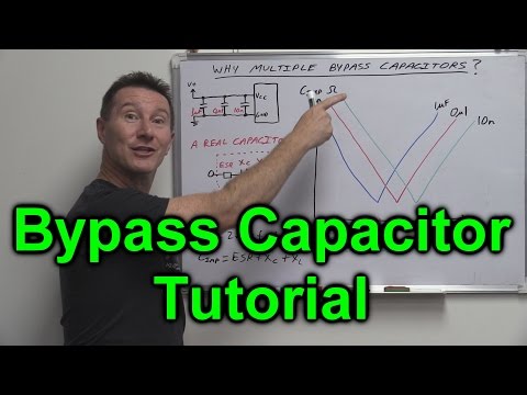
1 EEVblog #859 - Bypass / Decoupling Capacitor Tutorial
Dave Jones explains why decoupling capacitors are needed, how parasitics limit them, and why mixing values in parallel is not as simple as adding capacitance.
Topic
17 videos. Ranked by independent recommendations, not by views.
Dave Jones explains why decoupling capacitors are needed, how parasitics limit them, and why mixing values in parallel is not as simple as adding capacitance.
Rick Hartley's talk on grounding and return current paths in PCB design, praised as dense with practical EMC insight that formal courses often miss.
Dave Jones measures how much solder over exposed traces lowers resistance, finding roughly a 50 percent cut on 1 oz copper; cited for high current PCB traces.
Dave Jones visualises bypass capacitor behaviour; usually linked alongside his bypass tutorial when people ask how to choose values and place decoupling capacitors.
Rick Hartley's talk on routing differential pairs, recommended for understanding reference planes, return currents and termination at high speeds.
A w2aew demonstration of why boards use several decoupling capacitors of different values in different places, and what that does to the supply rails.
Rick Hartley explains how to order, pour and couple PCB layers, with recommended four, six and eight-layer stackups that pair every signal and power layer with ground.
Measures how much adding solder to high-current PCB tracks lowers resistance, finding about 30 per cent; cited alongside Dave Jones's similar test in track-width discussions.
Eric Bogatin's AltiumLive talk challenges inherited PCB rules, cited for why mixed-value decoupling capacitors are outdated with surface-mount parts and why signal-layer ground pour can hurt.
Jeremy Blum's second Eagle tutorial covers laying out and routing a printed circuit board; first-time designers follow it for their first boards before sending them to a fab.
Rick Hartley's long talk on controlling noise and EMI in circuit boards; cited on electronics.stackexchange.com for edge stitching vias and why rise time, not bit rate, sets bandwidth.
Hidden gemDave Jones explains PCB spark gaps; cited in discussions of spark gaps and gas discharge tubes as protection against high-voltage transients.
Eric Bogatin explains with Robert Feranec where return current really flows and why split planes cause trouble; repeatedly recommended for anyone routing signals between layers.
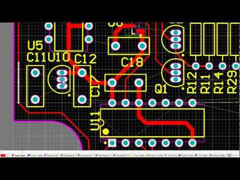
Hidden gemDave Jones laying out a real power supply board, often named as the main video to watch for PCB layout best practice once a schematic exists.
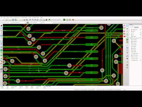
A demonstration of the KiCad interactive push and shove router from the CERN developers, linked to show how tracks can be dragged and rerouted in OpenGL mode.
Dave Jones on getting heat out of surface mount parts through the board, recommended for understanding thermal resistance and the electrical analogy for heat flow.
A PCB design tutorial that a student who picked up PCB skills from YouTube calls amazing and highly recommends to anyone starting out.